
Electroless Plating on Plastic
Plating & metallizing on plastics · Electroless (autocatalytic)
Electroless plating deposits nickel or copper uniformly on catalytically activated plastics and sealed 3D prints without external current.
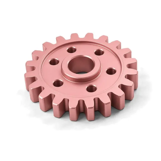
What is Electroless plastic?
It creates a conductive 5–15 µm metal layer for EMI shielding, further electroplating, or functional surfaces.
How it works
The polymer is cleaned, etched or otherwise roughened, sensitized, and activated with catalytic nuclei. An autocatalytic bath then reduces copper or nickel over all wetted activated surfaces without electrical current. Printed parts must first be cured, smoothed, and sealed. The metal layer can serve as the final functional film or as a conductive base for thicker electrolytic plating.
Why specify it
- Uniform 5–15 µm coverage
- Coats complex wetted geometry
- Makes plastic conductive
- Suitable base for later electroplating
Where it falls short
- Chemistry-specific properties vary
- Porous prints require sealing
- Bath access and drainage are essential
- Metal cannot strengthen a weak print core
Electroless plastic at a glance
Electroless plastic is a middle-of-the-range finish; its best score is cosmetic quality (60 of 100), at a high cost.
Each score is 0–100 against every finish in this catalog. Corrosion comes from salt-spray life (ASTM B117, log scale) and hardness from the finish layer's Vickers or pencil hardness; cosmetic, lubricity and cost are FabDigit's engineering assessment. Economy on the radar is the inverse of cost.
Electroless plastic key numbers
Typical values from the governing specifications and shop practice; bars are this finish against the highest value among plating & metallizing on plastics finishes.
- Thickness
- 5–10 µm functional seed or shielding layer
- Hardness
- 80–150 HV — Matches the copper-seed callout; electroless nickel on plastic is typically 400–600 HV as plated and must be specified separately.
- Electrical
- Conductive
- Colours
- copper
- silver
- gold-toned nickel
- Appearance
- Metallic copper or nickel; substrate texture remains visible unless filled and polished first.
Where Electroless plastic sits among all finishes
Surface hardness (Vickers, log scale) against corrosion protection (salt-spray hours, log scale) for every coating FabDigit offers, one cloud per finish group. Electroless plastic is highlighted; hover a dot for its name or open the full map.
Specifications for Electroless plastic
The documents a drawing cites to define this finish, with the Type / Class rows that apply. Each links to a page explaining the standard.
Drawing call-out
ELECTROLESS DEPOSIT COPPER ON DESIGNATED SEALED POLYMER SURFACES, 8–12 µm THICK; SHEET RESISTANCE 0.05 Ω/SQ MAX; MASK SNAP FITS AND BONDING SURFACESWhich materials take Electroless plastic?
Verdict per material family, with the grades that behave differently. Each family links to its datasheets in the material library.
| Material family | Verdict | Notes |
|---|---|---|
| Yes | Chemistry must match resin and surface preparation. | |
| With care | Expose no fibers and qualify adhesion. | |
| With care | Seal porosity and verify layer adhesion before plating. | |
| With care | Seal powder-bed porosity before activation. | |
| With care | Fully cure, smooth, and seal before activation; adhesion is resin-specific. | |
| With care | Strong sealing is required on powder-bed nylon. | |
| No | This process is specified for polymers, not bulk aluminum. | |
| No | This process is specified for polymers, not brass. | |
| No | This process is specified for polymers, not copper alloys. | |
| No | Metal AM uses conventional electroless plating on metal, not this polymer process. | |
| No | This process is specified for polymers, not magnesium. | |
| No | This process is specified for polymers, not stainless steel. | |
| No | This process is specified for polymers, not steel. | |
| No | This process is specified for polymers, not titanium. | |
| No | This process is specified for polymers, not zinc alloys. |
How Electroless plastic is applied, and what it does to the part
- 1Cure, clean, and seal
- 2Etch or roughen
- 3Sensitize and activate
- 4Electroless copper or nickel deposition
- 5Rinse and post-treat
- 6Test adhesion and resistance
| Dimensions | A 5–15 µm layer coats recesses as well as outside surfaces; total diametral change can be twice the deposit thickness. |
|---|---|
| Build-up per side | 5–15 µm — Allow full deposit thickness on all activated wetted surfaces. |
| Masking | Usually needed. Mask bonding, threads, snap fits, RF keep-outs, and non-conductive zones before activation. |
| Electrical | Conductive |
| Temperature limit | 100 °C (212 °F) continuous |
| Appearance | Metallic copper or nickel; substrate texture remains visible unless filled and polished first. |
| Added lead time | 10–20 working days on top of the bare part |
Design rules for Electroless plastic
What to decide on the drawing before the part goes to the finisher.
- Name copper or nickel chemistry.Generic electroless plating has no single hardness or conductivity.
- Seal additive parts completely.Bath entrapment and outgassing ruin adhesion.
- Provide drain paths.All wet processes must rinse cleanly.
- Specify sheet resistance for EMI use.Thickness alone does not prove electrical continuity.
Electroless plastic versus the alternatives
Finishes engineers weigh against Electroless plastic, and when each wins.
| Finish | Corrosion | Hardness | Cosmetic | Cost | Thickness | Choose it when |
|---|---|---|---|---|---|---|
Electroless plastic this page | 58 | 39 | 60 | $$$$ | 5–15 µm | — |
| 45 | — | 94 | $$$$ | 0.05–1 µm | reflective appearance with minimum metal thickness is wanted | |
| 72 | 71 | 98 | $$$$ | 20–50 µm | a complete decorative Cu-Ni-Cr stack is required |
The radar overlays Electroless plastic with Vacuum Metallization, its most common alternative — chosen reflective appearance with minimum metal thickness is wanted. Scores in the table are 0–100 across every finish in the catalog.
Cost, lead time and compliance
Relative cost
Electroless Plating on Plastic is a high-cost finish ($$$$): more expensive than about 75 % of the finishes FabDigit quotes.
Finishing is priced per part with a lot minimum, from FabDigit's own China-side rates. The exact figure appears on the instant quote once the part is uploaded.
Lead time and compliance
| Added lead time | 10–20 working days |
|---|---|
| RoHS | Compliant |
| Notes | RoHS-compliant deposits are available; bath reducers, complexants, and metal-bearing wastewater require treatment. |
What Electroless plastic is used for
- EMI-shielded housings
- Conductive 3D-printed prototypes
- Plating seed layers
- RF enclosures
Electroless plastic — frequently asked
Can plastic be electroless plated?
Yes after etching or roughening and catalytic activation. The autocatalytic bath then deposits metal without connecting the part to electrical current.
Can 3D prints be metal plated?
Yes, but resin must be fully cured and porous prints must be sealed. Surface texture remains visible unless it is filled and polished first.
How thick is electroless plating on plastic?
A functional seed or shielding layer is commonly 5–15 µm. Additional electrolytic copper or nickel can make the total stack much thicker.
Electroless copper vs electroless nickel on plastic?
Copper offers high electrical conductivity and is a common EMI or electroplating base. Nickel offers better wear and barrier behavior but chemistry-specific data must be specified.
Does electroless plating coat inside features?
It coats activated surfaces reached and refreshed by solution more uniformly than electrolytic plating. Blind cavities still need drainage and bath circulation.