
Electroless Copper Plating
Electroplating & electroless plating · Electroless (autocatalytic)
Electroless copper chemically deposits a conductive seed layer on catalyzed plastics and inside printed-circuit through-holes.
Reference page — Electroless copper is not in the instant-quote configurator. Upload the part, name the finish in the notes, and an engineer quotes it with the part.
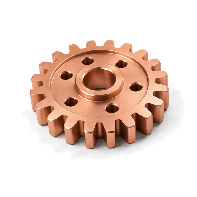
What is Electroless copper?
Electrolytic copper normally follows when greater thickness is required.
How it works
The surface is cleaned, conditioned, etched where necessary, and seeded with a catalyst such as palladium. In an alkaline bath, a reducing agent converts dissolved copper ions to metal on the catalytic surface without external current. Once deposition starts, copper catalyzes further growth. Coverage is more uniform than electrolytic plating, including through-holes, but bath stability and solution exchange limit practical build rate and thickness.
Why specify it
- Makes nonconductive surfaces electrically conductive
- Uniform 0.2–5 µm seed coverage
- Reaches through-holes without current
- Enables later electrolytic copper, nickel, or chrome
Where it falls short
- Bath is chemically unstable and tightly controlled
- Thin seed layer is not a durable final finish
- Poor cleaning causes skip plating
- Deep blind cavities still need solution exchange
Electroless copper at a glance
Electroless copper is a middle-of-the-range finish; its best score is cosmetic quality (42 of 100), at a premium cost.
Each score is 0–100 against every finish in this catalog. Corrosion comes from salt-spray life (ASTM B117, log scale) and hardness from the finish layer's Vickers or pencil hardness; cosmetic, lubricity and cost are FabDigit's engineering assessment. Economy on the radar is the inverse of cost.
Electroless copper key numbers
Typical values from the governing specifications and shop practice; bars are this finish against the highest value among electroplating & electroless plating finishes.
- Thickness
- 0.2–1 µm seed layer for through-holes; 1–5 µm for plastics metallization before electrolytic build
- Hardness
- 80–200 HV — Deposit properties depend on bath chemistry and incorporated impurities.
- Electrical
- Conductive
- Colours
- copper
- Appearance
- Uniform matte pink copper seed layer, normally hidden by subsequent electroplating.
Where Electroless copper sits among all finishes
Surface hardness (Vickers, log scale) against corrosion protection (salt-spray hours, log scale) for every coating FabDigit offers, one cloud per finish group. Electroless copper is highlighted; hover a dot for its name or open the full map.
Specifications for Electroless copper
The documents a drawing cites to define this finish, with the Type / Class rows that apply. Each links to a page explaining the standard.
Drawing call-out
ELECTROLESS COPPER SEED LAYER, 1–3 µm, CONTINUOUS ON ALL INDICATED PLASTIC SURFACES AND THROUGH-HOLES; FOLLOW WITH 20 µm MIN ELECTROLYTIC COPPERWhich materials take Electroless copper?
Verdict per material family, with the grades that behave differently. Each family links to its datasheets in the material library.
| Material family | Verdict | Notes |
|---|---|---|
| With care | Possible after specialized sensitization and activation. | |
| With care | Adhesion depends on matrix and exposed reinforcement. | |
| Limited | Not a first-choice aluminum finish; zincate plus electrolytic or electroless nickel is more common. | |
| Limited | Rarely specified as a standalone brass finish. | |
| Limited | Rarely needed on already-conductive copper alloys except as a seed in mixed assemblies. | |
| Limited | Metal AM parts do not need electroless copper except as a specialized seed. | |
| Limited | Only plateable resins after etch and catalysis. | |
| Limited | Porous nylon is difficult to seal and catalyze uniformly. | |
| Limited | Requires plateable resin and qualified etch/catalyst process.
| |
| Limited | Only qualified photopolymers after etch and catalysis. | |
| Limited | Porous nylon is difficult to seal and catalyze uniformly. | |
| Limited | Requires aggressive activation; other metallization routes are more common. | |
| Limited | Used mainly as a thin seed or strike, not a standalone engineering coating. | |
| Limited | Possible as part of a plastic/metal metallization stack after a strike. | |
| No | Too reactive for a standard electroless-copper cycle. | |
| No | Titanium is not a routine electroless-copper substrate. |
How Electroless copper is applied, and what it does to the part
- 1Clean and condition
- 2Etch
- 3Neutralize
- 4Catalyze
- 5Accelerate
- 6Electroless copper deposit
- 7Rinse
- 8Electrolytic build or inspect
| Dimensions | Initial buildup is only 0.2–5 µm per side; include all subsequent electrolytic layers in finished dimensions. |
|---|---|
| Build-up per side | 0.2–5 µm — Chemical deposition is relatively uniform; later electrolytic copper adds nonuniform buildup. |
| Masking | Usually needed. Mask all areas that must remain insulating because catalyst carryover can cause unwanted metal growth. |
| Electrical | Conductive |
| Appearance | Uniform matte pink copper seed layer, normally hidden by subsequent electroplating. |
| Added lead time | 4–8 working days on top of the bare part |
Design rules for Electroless copper
What to decide on the drawing before the part goes to the finisher.
- Use a plateable polymer and qualified etch.Adhesion depends on controlled micro-roughening and catalyst retention.
- Keep masked areas free of catalyst.Residual catalyst causes unwanted copper islands.
- Provide through-flow in holes.Fresh bath must reach every catalytic surface.
- Specify the complete metal stack.A 0.2–5 µm seed is not a durable final coating.
Electroless copper versus the alternatives
Finishes engineers weigh against Electroless copper, and when each wins.
| Finish | Corrosion | Hardness | Cosmetic | Cost | Thickness | Choose it when |
|---|---|---|---|---|---|---|
Electroless copper this page | 20 | 41 | 42 | $$$ | 0.2–5 µm | — |
| 32 | 39 | 65 | $$ | 5–30 µm | when an already conductive substrate needs faster, thicker buildup | |
| 70 | 68 | 55 | $$$ | 5–75 µm | when a harder uniform final coating is required |
The radar overlays Electroless copper with Copper Plating, its most common alternative — chosen when an already conductive substrate needs faster, thicker buildup. Scores in the table are 0–100 across every finish in the catalog.
Cost, lead time and compliance
Relative cost
Electroless Copper Plating is a premium-cost finish ($$$): more expensive than about 67 % of the finishes FabDigit quotes.
Finishing is priced per part with a lot minimum, from FabDigit's own China-side rates. The exact figure appears on the instant quote once the part is uploaded.
Lead time and compliance
| Added lead time | 4–8 working days |
|---|---|
| RoHS | Compliant |
| Notes | Copper is RoHS compatible; reducing agents, complexants, catalyst metals, and copper wastewater require controlled treatment. |
What Electroless copper is used for
- Plating-on-plastic seed layers
- PCB through-holes
- EMI shielding
- Metallized prototypes
Electroless copper — frequently asked
electroless copper vs electrolytic copper
Electroless copper deposits without current and uniformly seeds plastics and through-holes at about 0.2–5 µm. Electrolytic copper needs a conductive path, deposits faster, and commonly builds 5–30 µm or more.
can you copper plate plastic
Yes, a plateable plastic is etched, catalyzed, and electrolessly coated with roughly 1–5 µm of copper. Electrolytic copper and final nickel, chrome, or other layers then provide thickness and durability.
how thick is electroless copper
PCB seed layers can be about 0.2–1 µm, while plating-on-plastic base layers often use 1–5 µm. Heavy final copper is normally built electrolytically.
how does through hole copper plating work
Catalyst activates the nonconductive hole wall, and electroless copper creates a continuous conductive film, often 0.2–1 µm. Electrolytic copper then increases wall thickness.
is electroless copper a final finish
Usually no; the thin seed oxidizes and lacks wear resistance. It is normally buried under thicker copper, nickel, chrome, or another functional topcoat.
Other electroplating & electroless plating finishes
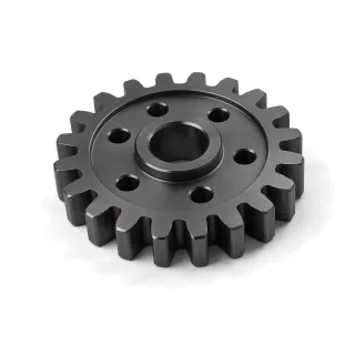 Black Nickel PlatingBlack nickel is a thin dark decorative electrodeposit, commonly applied over nickel, copper, brass, or zinc.CorrosionHardnessCost$$$
 Brass PlatingBrass plating co-deposits copper and zinc to give steel, zinc die castings, or copper alloys a yellow decorative surface.CorrosionHardnessCost$$$
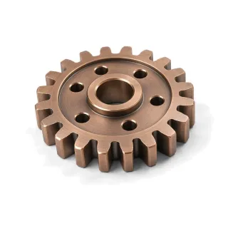 Bronze PlatingBronze plating deposits a copper-tin or related copper alloy for warm decorative color, antiquing, or selected functional bearing surfaces.CorrosionHardnessCost$$$
 Cadmium PlatingCadmium is a sacrificial, lubricious coating retained mainly for aerospace, defense, and legacy hardware.CorrosionHardnessCost$$$$
 Decorative Nickel-Chrome PlatingDecorative chrome is a multilayer system: copper when needed, one or more nickel layers, and a very thin chromium topcoat.CorrosionHardnessCost$$$
 Electrolytic Nickel PlatingElectrolytic nickel provides a bright decorative surface, corrosion barrier, wear layer, or undercoat for chromium and precious metals.CorrosionHardnessCost$$
 Gold PlatingGold plating supplies tarnish-free, low-resistance contact surfaces and decorative color.CorrosionHardnessCost$$$$
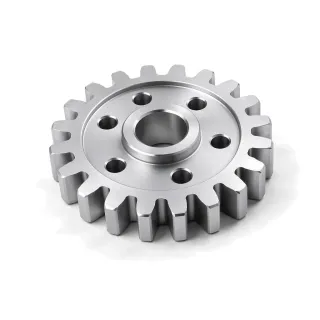 Hard Chrome PlatingHard chrome is a thick engineering chromium deposit for wear, low friction, and dimensional restoration.CorrosionHardnessCost$$$$
Compare every electroplating & electroless plating finish side by side →