
Gerbers in.
Boards out.
Assemblies ready.
Quick-turn PCB fabrication and PCBA assembly — 24-hour prototypes, low-volume production, and turnkey BOM sourcing. SMT, through-hole, mixed, BGA rework, conformal coating, and ICT/AOI all under one program engineer.
Veteran program leads
Programs run by engineers who have shipped real boards at production scale.
Quoted in hours
Every quote comes with engineer review and DFM notes — not just a price.
FAI on every order
Every order ships with a full first-article AOI / ICT report against your CAD.
Direct engineer access
Email, call, or video — talk straight to the person running your job.
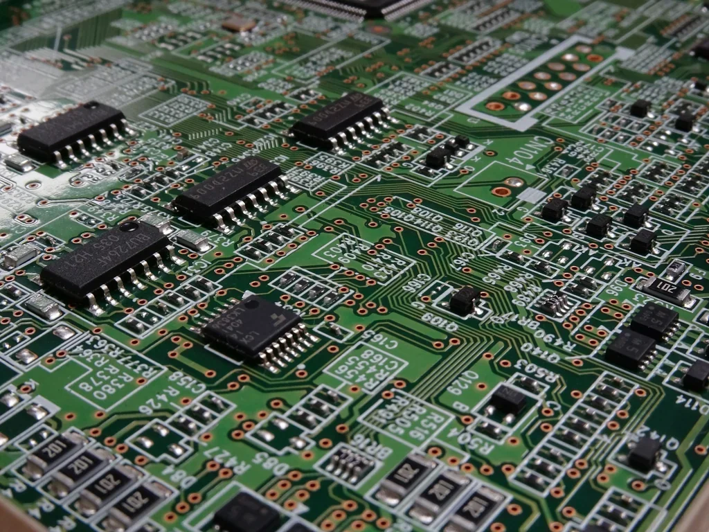
Six processes, one program engineer.
Bare-board fab and PCBA assembly run side-by-side, plus the specialty processes that turn a populated panel into a shippable product. One quote covers the whole chain.
PCB fabrication
Bare-board build — 2 to 32 layers, FR-4 through Rogers and polyimide.
Boards in 24 h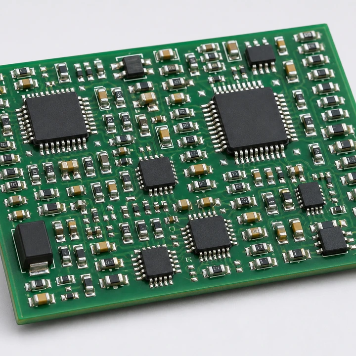
SMT assembly
Solder-paste stencil + pick-and-place + reflow. 0201 and µBGA capable.
0201 / µBGA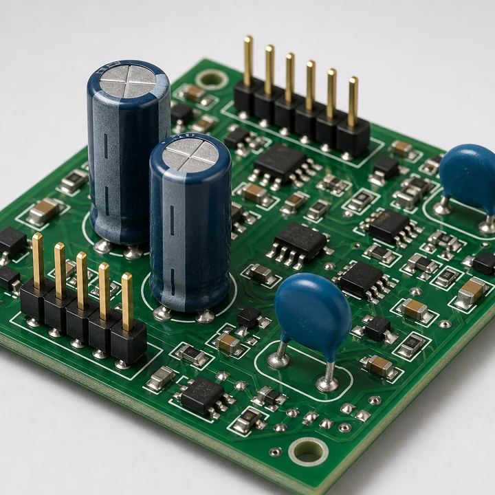
Through-hole + mixed
Selective and wave soldering for connectors, large caps, and heatsinks.
Mixed-tech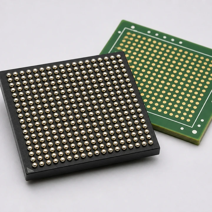
BGA / fine-pitch rework
X-ray inspection, hot-air station rework, ball-attach and reballing.
X-ray + rework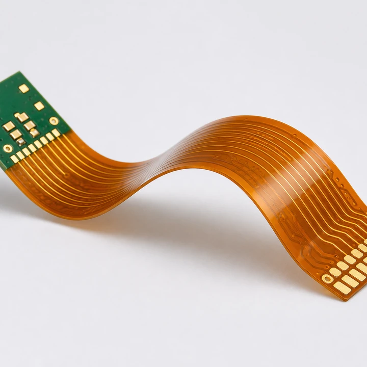
Flex + rigid-flex
Polyimide flex circuits, multi-layer rigid-flex with controlled impedance.
Polyimide flex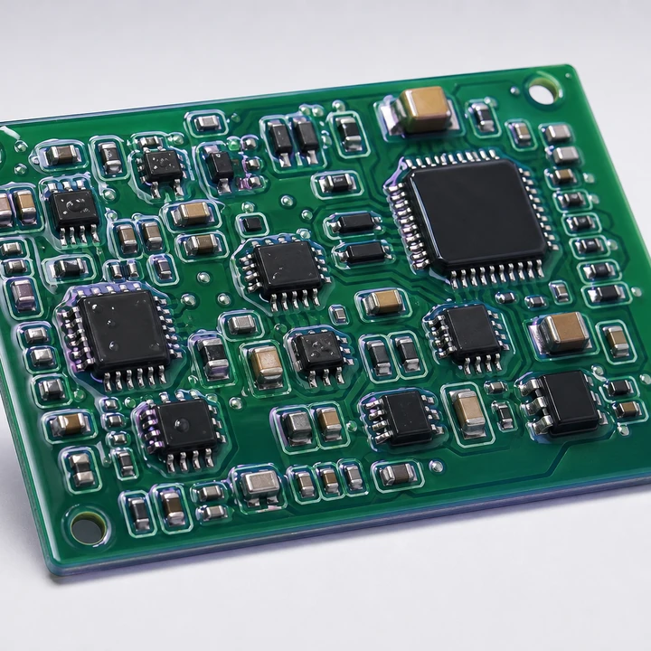
Conformal coating
Acrylic, silicone, urethane, parylene. UV-cure or solvent dip.
IPC-A-610 Class 3The full envelope.
Board size
5 × 5 mm → 600 × 600 mmStandard panel is 18 × 24". Larger panels available on request — 1.2 m × 1.5 m max.
Layer count
1 → 32 layers2-4 layer FR-4 is our highest-volume product. 16-32 layer HDI and rigid-flex on a different process line.
Board thickness
0.2 mm → 6.0 mm0.4 / 0.6 / 0.8 / 1.0 / 1.2 / 1.6 / 2.0 / 2.4 / 3.0 mm standard. Non-standard thickness available.
Copper weight
0.5 oz → 6 ozInner-layer 0.5 oz / outer 1 oz is the volume standard. 3 oz and above for high-current power planes.
Min trace / space
3 mil / 3 mil (HDI)4 mil / 4 mil standard. 3 mil / 3 mil HDI on advanced line. 6 mil / 6 mil is the high-yield sweet spot.
Min drill
0.10 mm laser / 0.15 mm mechanical0.20 mm is the high-yield mechanical drill. Laser-drilled microvias below 0.15 mm for HDI.
Impedance control
±5% on controlled linesSingle-ended 50 Ω, differential 90 Ω / 100 Ω. TDR coupon report shipped with the boards.
PCBA — components
0201 → BGA 0.3 mm pitchPick-and-place at 30 K CPH. Mixed SMT + through-hole + selective solder on one line.
PCBA — order quantity
1 → 100 KPrototype builds from a single board. Production runs scale to 100K with no tooling change.
IPC class
IPC-A-610 Class 2 / 3Class 3 (medical / aerospace) workmanship is the default for safety-critical boards.
See the board in cross-section.
Default is 4-layer FR-4 — the production-volume sweet spot. Pick a layer count to see how copper plane allocation and dielectric thicknesses shift, then tap any layer in the diagram for its role, copper weight, and thickness.
Cu L1
- Purpose
- Signal
- Thickness
- 1 oz · 35 µm
- Layer kind
- copper
Stack-ups shown here are representative — actual core / prepreg thicknesses are tuned to your impedance and finished-thickness targets at quote time. We can also build to your existing stack-up drawing without modification.
Where your design sits in our window.
Three concentric process bands: Standard for high-yield volume, Advanced for fine-pitch BGA breakout, HDI for laser-microvia and 3-mil trace. The chart below shows where each axis tightens up.
Trace widthmil
- Standard. 6 mil / 0.15 mm — high-yield, the volume default.
- Advanced. 4 mil / 0.10 mm — fine-pitch BGA breakout.
- HDI. 3 mil / 0.075 mm — HDI line, 75 µm laser-imaged.
Trace spacingmil
- Standard. 6 mil clearance — same line as trace standard.
- Advanced. 4 mil clearance — dense routing on FR-4.
- HDI. 3 mil — HDI line, controlled etch chemistry.
Min drill — mech.mm
- Standard. 0.20 mm — standard mech drill, finished hole 0.15 mm.
- Advanced. 0.15 mm — tightened drill cycle, 8 : 1 aspect.
- HDI. 0.10 mm laser microvia — blind / buried allowed.
FR-4 to ceramic — same engineer.
The catalogue below is what we keep on the floor or can pull within 48 hours from authorised distribution. Special high-frequency laminates (Taconic, Megtron, Nelco) and custom co-fire ceramics on request.
Need a laminate not shown above? Name it, send a manufacturer datasheet, and we will source it. Material certs and lot traceability included with every order.
Eight finishes, picked for the design.
ENIG is our default for fine-pitch SMT. OSP for cost-sensitive single-reflow. HASL for through-hole legacy. Each surface has its own trade-off — surfacing them up front avoids surprises at PCBA time.
Gerbers to door, in four steps.
Same engineer reviews the Gerbers, runs the BOM cross-ref, signs off on the stack-up, and inspects the first-article report — no handoffs between sales and production.
Upload Gerbers + BOM
Gerber 274X, IPC-2581, ODB++, or native Altium / KiCad. BOM in CSV / Excel.
DFM + IPC review
Stack-up, impedance, trace clearances, soldermask, BOM cross-ref — reviewed by an engineer in 4–24 hours.
Fab + assembly
Bare boards built; stencil cut; components placed; reflow + selective solder + ICT/AOI.
Test, FAI, ship
Flying-probe or fixtured ICT, AOI for cosmetics, X-ray for BGA. First-article report ships with the boards.
What is always included
- Free DFM review with every quote
- IPC-A-610 Class 2 or Class 3 workmanship
- AOI 100% of assembled boards
- X-ray inspection on BGA / QFN
- TDR impedance coupon with controlled boards
- BOM cross-ref + lifecycle check before procurement
- NDA before file upload — on request
- Direct engineer access — email, call, or video
Gerbers to populated board, day by day.
A typical 4-layer prototype build with 100 SMT placements. 2-layer rapid-line prototypes compress this to 3 days; 8-layer + HDI + Class 3 stretches it to 14 days.
Quote + DFM
Day 0 → 0.5Bare-board fab
Day 0.5 → 3BOM + stencil
Day 1 → 3PCBA + reflow
Day 3 → 5AOI / ICT / X-ray
Day 5 → 6FAI + ship
Day 6 → 7Rush 24-hour 2-layer prototype boards are available with surcharge. After the first build, repeat orders ship the bare boards from a held stack and rerun the PCBA in 2–3 days.
Answers, on the record.
Engineers wrote these. If yours is not here, emailengineering@fabdigit.com — typical reply within 4 business hours.
Gerber RS-274X (preferred), IPC-2581, ODB++, or native Altium / KiCad / Eagle. Centroid (pick-and-place) file and BOM in CSV or Excel for assembly. NC-drill and aperture files are auto-extracted from Gerber sets.
Yes for 2-layer FR-4 prototypes, in our rapid line. 4-layer 48 h. 6-layer 4 days. Same-day fab is available with surcharge on 2-layer boards. PCBA on top of fab adds 1–3 days depending on component sourcing and complexity.
Yes — full turnkey. We pull pricing from Digi-Key, Mouser, Avnet, Arrow, and authorised China distribution. Counterfeit-screened parts only. You see the BOM cross-ref + lifecycle status (active / NRND / EOL) before we commit to procurement. Consigned and partial-consigned builds are also supported.
Class 2 is the default for most consumer / industrial. Class 3 (medical / aerospace / automotive critical safety) is available on request — Class 3 workmanship is the same operators with stricter inspection criteria, not a different line. Class 3 documentation (FAI + traceability + lot records) is included in the Class 3 quote.
Yes — single-ended 50 Ω, differential 90 Ω / 100 Ω. We co-engineer the stack-up with your designer to hit the impedance target on the trace widths shown. A TDR impedance coupon ships with the order so you can verify the controlled-impedance lines before production.
6 mil trace + 6 mil space is the volume sweet spot. Down to 4 mil / 4 mil on the standard line, 3 mil / 3 mil on the advanced (HDI) line. Min mechanical drill 0.15 mm, min laser microvia 0.10 mm. Blind and buried vias supported.
Yes — 0.3 mm-pitch µBGA and 0201 passives are routinely placed. X-ray inspection (post-reflow) is included for all BGA / QFN assemblies. We have an in-house BGA rework station with hot-air + thermocouple control for repair and reballing.
Yes — single-layer to 4-layer flex, polyimide-based. Rigid-flex (multi-layer FR-4 cores stitched with polyimide flex sections) is supported up to 14 total layers. Send the stack-up; we will quote both the flex-only and the rigid-flex variants.
Yes. UL-94 V-0 flame-retardant base laminates are the default for FR-4. UL-recognised PCB shop mark can be silk-screened on production boards on request — the file mark is provided to you before fabrication.
Yes. Prototype runs from a single board are the most common starting point. Stencil + first-article + a hand-placed pilot is our default for the first 1–10 boards. Production at 100 to 100K runs on the SMT line without a tooling change.
From Gerbers to populated boards — same engineer.
Bare-board prototypes in 24 hours. Turnkey PCBA in a week. Programs run by people who have shipped boards.